Design and layout is an art form, and never more so than when you are designing an RF circuit.
SSS Online is proud to present some tricks and hints on this important topic to help you design RF circuits that don't fall prey
to the harmonics, drop out and other bugaboos that can haunt the designer.
Layout Considerations for Texas Instruments CC1100/1101 Transceiver
by Eric Myers, Senior RF Circuit Design Engineer, Pegasus
Technologies, Inc.
Introduction
One of the RF chips that we have used in many of our current designs is the Texas Instruments CC1100/1101 transceiver chip.
This chip is an inexpensive and very versatile sub-1GHz transceiver that is aimed at ultra-low power wireless applications in a variety of frequency bands. The versatility of this
chip is enhanced by its integrated and highly configurable baseband modem, which supports a number of different modulation formats and data rates. With extensive capabilities for
packet handling, data buffering, burst transmissions, clear channel assessment, and link quality indication, this chip is typically used with an on-board microcontroller.
Originally developed by ChipCon, this chip has continued as an active TI product following their acquisition of ChipCon in early 2006. The newest version of this chip, the
CC1101, has been recently introduced and is the chip we are using in new designs.
The pin-for-pin and code compatible CC1101 has better spurious response and improved close-in phase noise for adjacent channel performance.
We selected the CC1100/1101 for our designs due to its versatility and small form factor. We typically pair it with the MSP430 microcontroller, a decision we made before TI's
acquisition of Chipcon and which works especially well now that both are manufactured by the same company. This microcontroller, an ultra-low-power 16-bit RISC mixed-signal
processor, is ideal for low power and portable applications. TI has also combined the 1100 with an 8051 MCU to create a system-on-chip IC (CC1110), and is in the process
of developing an IC with the 430 MCU. This provides us with the ability to offer several options to our clients while using a consistent and proven transceiver architecture.
In designing circuits using their components, Texas Instruments' website provides very helpful documentation and design examples. TI also continuously works to improve
their reference designs. At the present time (August 2009), three designs have been published for the CC1100 chip, but the first two are no longer recommended. The
current design has improvements to eliminate harmonic emission as well as variations based on power settings. Some of the older data sheets still show the older
designs, however, so RF engineers using this chip should be sure to download the most recent version from the TI website when beginning a new design. The current
version at the time this article was written is Rev D, dated May 29, 2009.
The current version for the CC1101 is CC1101: Low-Power Sub-1 GHz RF Transceiver (Enhanced CC1100), of 2009.
Although TI's datasheets are invaluable in incorporating this chip into a particular design, we have still found some issues that are not addressed, particularly
related to layout, and have written this article to fill in some of the gaps based on our own experience.
Filter Topology and Layout Concerns
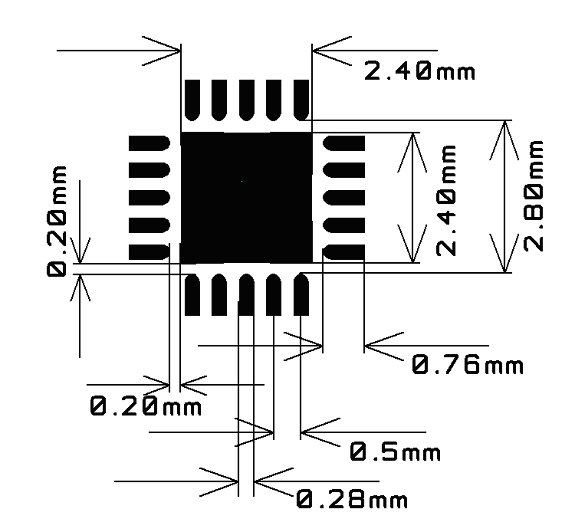
TI shows a recommended layout for the CC1100 on page 89 of its datasheet. A copy of the picture is reproduced below:
Recommended PCB Layout for QLP 20 Package
TI notes that this diagram is an illustration only and not to scale, and that there are five 10 mil via holes distributed symmetrically in the ground pad
under the package that are not shown in the diagram. What the picture does not show is how the supporting components should be placed and routed. The
following sections will provide descriptions of the more important sections along with pictures showing the recommended and not recommended ways of configuring them.
Filter Topology
One of the key pieces of a design using the CC1100 is the filter balun. The design of the filter balun accomplishes three main tasks. First it converts the
balanced RF signals from the CC1100 into an unbalanced signal. Second it provides a low pass filter. The third task is to match the impedance from the
output of the CC1100 to the impedance of the antenna (typically 50Ω). Because of the importance and multi-tasking required by this portion of the design,
there are some important considerations in layout that need to be taken into account.
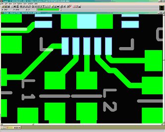
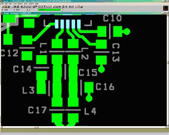
The balanced portion of the filter balun is very susceptible to variations between the two sections. For this reason, it is very important to keep the
component spacing and traces as equal as possible. As an example, when placing the LPF inductors that connect directly to the CC1100, it would be better
to have both set slightly off from the pins. This would allow for the traces to be of equal length and shape. If one inductor is placed so that it has a
very short straight trace, the other inductor will not fit in front of its corresponding pin. This will cause the trace for the second inductor to be
longer with more bending. The effect of having the two sides with uneven layouts is higher harmonics (especially the 2nd and 4th) as well as reduced
output power at the single-ended side of the filter balun.
Figure 1-Incorrect
Figure 2-Correct
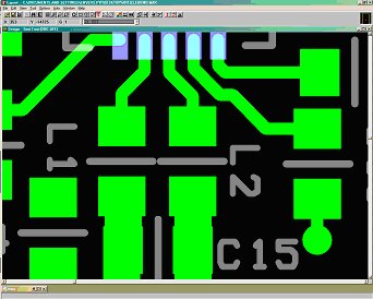
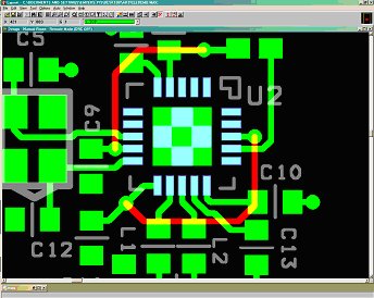
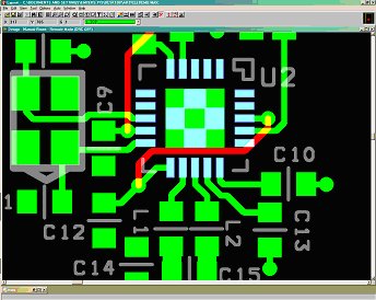
The single-ended side of the filter balun is designed to be 50Ω impedance. The trace width for this section up to the antenna should be 50Ω. However, the
trace widths for the filter balun section itself should be as wide as possible without requiring a resize at the pads of the filter balun components
(in other words, you should make the traces from the CC1100 to the filter inductors the same width as the CC1100 pads). In and ideal world, the
components would be right next to each other without any traces required to connect them. However since that is not possible, the next best approach
is to minimize the amount of inductance within the trace by making it as wide as possible based on the size of the component pads.
Figure 3-Incorrect
Figure 4-Correct
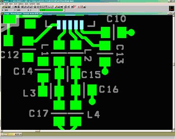
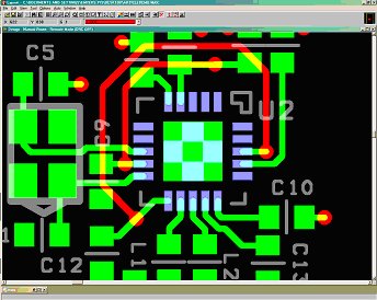
Solid ground plane below the IC and filter balun components
Another important aspect of the filter balun layout is the ground plane. The layer directly below the components should be a solid ground.
Because the CC1100 packaging has pins on all four sides, it can be difficult to connect things such as power. It is often necessary to
switch between layers in order access all of the connections required. With a multi-layer board, the first inner layer can be a solid
plane, which will accomplish this requirement rather easily. With a two-layer design, it becomes more complicated to achieve a solid
ground. The preferred method is to route bottom side traces on the opposite side of the CC1100 from the RF outputs. If this is not
possible, the trace should be routed directly below the device, but NOT under the RF pads or filter balun.
Figure 5-Incorrect
Figure 6 - Acceptable
Figure 7 - Correct
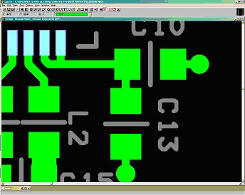
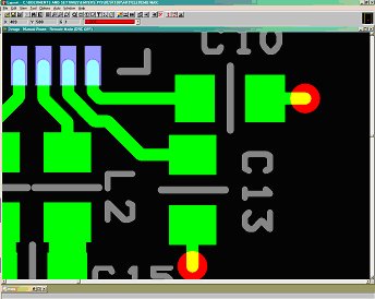
Importance of decoupling capacitors to each pin
When using the reference design provided by TI, it is important to understand that each decoupling component is included for a reason.
When pins are located next to each other and have a capacitor associated with each one, these components must be connected individually.
Do not simply connect the two pins together and then route a single trace to the two capacitors. By using a single trace the pins are no
longer isolated from each other. The correct procedure is to route an individual trace from each pin to its associated capacitor. This
will obviously make the layout a little more complicated, but extra effort will be appreciated when the circuit performs as expected
without troubleshooting and modifications to the PCB.
Figure 8-Incorrect
Figure 9-Correct
Trace width variation with different PCB thicknesses
At the output of the filter balun, the RF output is now 50Ω impedance. The trace width needs to be set based on the thickness of the
dielectric and maintained up to the antenna. In this case, if the width is wider than the component pads, the trace will have to be
reduced just before entering the pad. As with the filter balun section, the ground plane below the trace must be solid up to the
antenna. Depending on the style of antenna, the ground plane may or may not need to be removed at the antenna itself.
Conclusion
This article, if read in conjunction with the excellent TI application notes for this chip, will make it easier to incorporate the
CC1100 into your design. While the advice presented here may seem simple, failure to apply these techniques may result in a circuit
that does not perform as desired. By taking the time apply these techniques, hopefully, it will save you some layout mistakes and
reworks, and thus reduce both development time and costs. You can spend all this time and money you save here on designing better
firmware for the chip and its associated microcontroller - with the versatility available with the CC1100, this is where the real
excitement should be!
TI Developer's Network.
We are proud to be a member of the Texas Instruments' Low Power RF developer's network.
Design Bureau Listings.
Pegasus Technologies, in conjunction with our subsidiary Design Sources, is listed as an EMA Design
Automation Service Bureau using Cadence Allegro Design Software.
We are also listed as an Altium Service Bureau using the latest Altium Designer
PCB design software with the Extended Feature Set. This service is also offered in conjunction
with Design Sources.
Low Power Design — a site aimed at engineers that creates and aggregates
design news and articles "to help power the green revolution.". Don't let that stop you, there are still some good articles here!